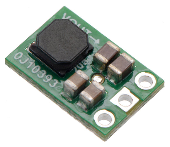
This compact step-up (or boost) regulator generates 5 V from voltages as low as 0.8 V and delivers up to 200 mA, making it perfect for powering small 5 V electronics projects from 1 to 3 NiMH, NiCd, or alkaline cells or from a single lithium-ion cell.
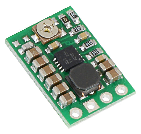
These tiny boost (step-up) switching regulators are based on the NCP1402 boost regulator IC. Their small dimensions of just 0.33″ × 0.5″ (8.4 mm × 12.7 mm) and a startup voltage of down to 0.8 V make it easy to build 3.3 V and 5 V circuits that are powered by lower battery voltages. The available output current and output voltage ripple depend on the input voltage, but the regulator can provide up to 200 mA if the input voltage is high enough.
With low input voltages, the output voltage ripple is under 40 mV peak-to-peak. When the input voltage is close to the output, the output ripple quickly climbs to 150 mV peak-to-peak. Therefore, adding capacitance from the output to ground is recommended for noise-sensitive applications with input voltages close to the output voltage.
Some example applications include:
- Powering 3.3 V or 5 V systems from lower-voltage batteries.
- Powering higher-voltage subsystems in lower-voltage systems (e.g. powering a 5 V sensor in a 3.3 V system).
This regulator is available with a fixed 3.3 V or 5 V output.
For higher-power applications, consider using one of our adjustable boost regulators or our U3V12Fx boost regulators.
Using the Boost Regulator
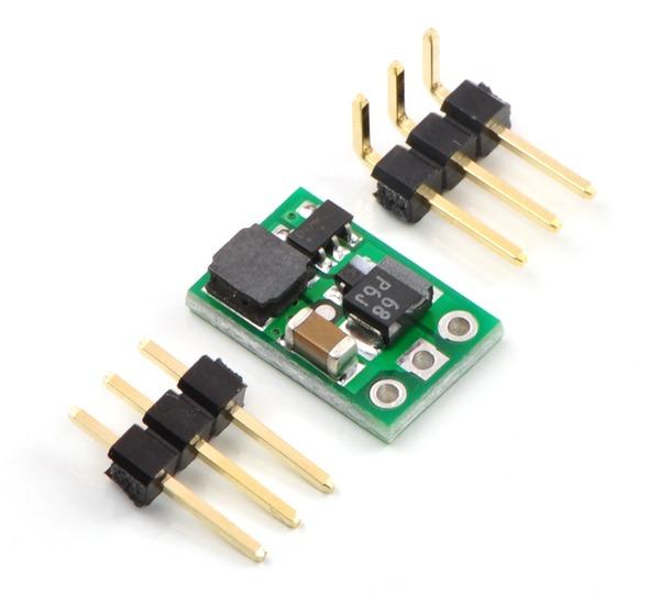
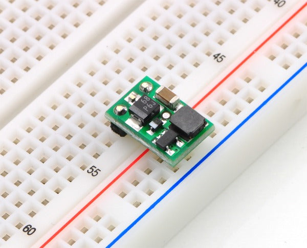
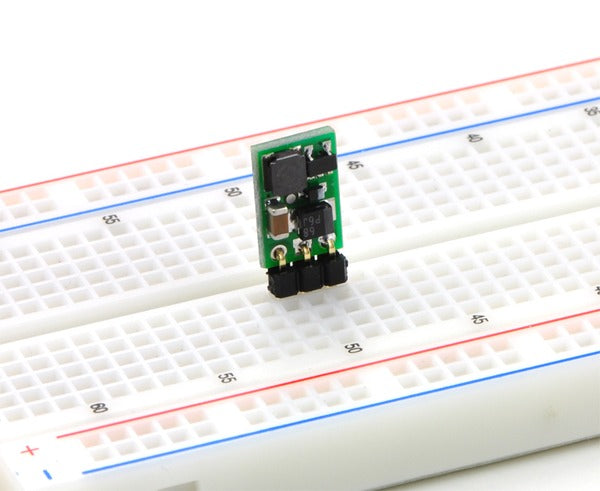
The boost regulator has just three connections: the input voltage, ground, and the output voltage. These three connections are labeled on the back side of the PCB and they are arranged with a 0.1″ spacing along the edge of the board for compatibility with standard solderless breadboards and perfboards and connectors that use a 0.1″ grid. You can solder wires directly to the board or solder in either the 3×1 straight male header strip or the 3×1 right-angle male header strip that are included.
Feature summary
- Operating voltage: 0.8 V – VOUT
- 3.3 V or 5.0 V output with 2.5% accuracy
- <3 mA typical no-load quiescent current
- Small size: 8.4 mm × 12.7 mm × 3.8 mm (0.33″ × 0.50″ × 0.15″)
- Weight without header pins: 0.6 g (0.02 oz)
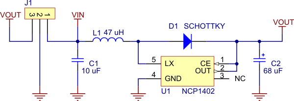
 |
| 5V boost regulator NCP1402 schematic diagram. |
|---|
Typical Efficiency and Output Current
The efficiency of a voltage regulator, defined as (Power out)/(Power in), is an important measure of its performance, especially when battery life or heat are concerns. As shown in the graphs below, this switching regulator typically has an efficiency of 75% to 90%.
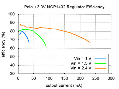

The maximum achievable output current is approximately proportional to the ratio of the input voltage to the output voltage. With a 0.8 V input, approximately 5 mA are available before the output voltage begins dropping. The full 200 mA output can be realized from input voltages over approximately 2.4 V (3.3 V version) or 2.7 V (5 V version). Additionally, the maximum output current can depend on other factors, including the ambient temperature, air flow, and heat sinking.
LC Voltage Spikes
When connecting voltage to electronic circuits, the initial rush of current can cause damaging voltage spikes that are much higher than the input voltage. In our tests with typical power leads (~30″ test clips), input voltages above 4 V caused voltage spikes in excess of 6 V, the absolute maximum voltage of the NCP1402. You can suppress such spikes by soldering a 33 μF or larger electrolytic capacitor close to the regulator between VIN and GND.