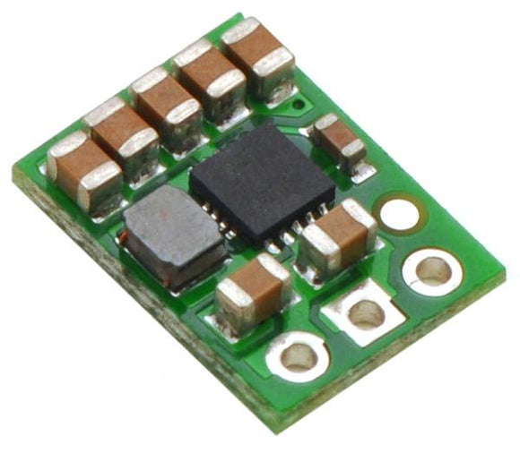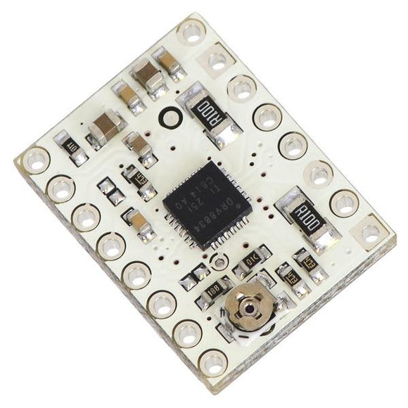


This tiny breakout board for TI’s DRV8835 dual motor driver can deliver 1.2 A per channel continuously (1.5 A peak) to a pair of DC motors, and it supports two possible control interfaces for added flexibility of use: IN/IN and PHASE/ENABLE. With an operating voltage range from 2 to 11 V and built-in protection against reverse-voltage, under-voltage, over-current, and over-temperature, this driver is a great solution for powering up to two small, low-voltage motors. The carrier board has the form factor of a 14-pin DIP package, which makes it easy to use with standard solderless breadboards and 0.1″ perfboards.
Texas Instruments’ DRV8835 is a tiny dual H-bridge motor driver IC that can be used for bidirectional control of two brushed DC motors at 2 to 11 V. It can supply up to about 1.2 A per channel continuously and can tolerate peak currents up to 1.5 A per channel for a few seconds, making it an ideal driver for small motors that run on relatively low voltages. The DRV8835 is a great IC, but its small, leadless package makes it difficult for the typical student or hobbyist to use; our breakout board gives this driver the form factor of a 14-pin DIP package, which makes it easy to use with standard solderless breadboards and 0.1″ perfboards. Since this board is a carrier for the DRV8835. The board ships populated with SMD components, including the DRV8835, and adds a FET for reverse battery protection.
This board is very similar to our DRV8833 dual motor driver carrier in operating voltage range and continuous current rating, but the DRV8835 has a lower minimum operating voltage, offers an extra control interface mode, and is 0.1″ smaller in each dimension. The DRV8833 has a higher peak current rating (2 A per channel vs 1.5 A), optional built-in current-limiting, and no need for externally supplied logic voltage.
For a higher-voltage alternative to this driver, please consider our DRV8801 motor driver carrier.
Features
- Dual-H-bridge motor driver: can drive two DC motors or one stepper motor
- Motor supply voltage: 2–11 V
- Logic supply voltage: 2–7 V
- Output current: 1.2 A continuous (1.5 A peak) per motor
- Motor outputs can be paralleled to deliver 2.4 A continuous (3 A peak) to a single motor
- Two possible interface modes: IN/IN (outputs mostly mirror inputs) or PHASE/ENABLE (one pin for direction and another for speed)
- Inputs are 3V- and 5V-compatible
- Under-voltage lockout and protection against over-current and over-temperature
- Reverse-voltage protection on the motor supply
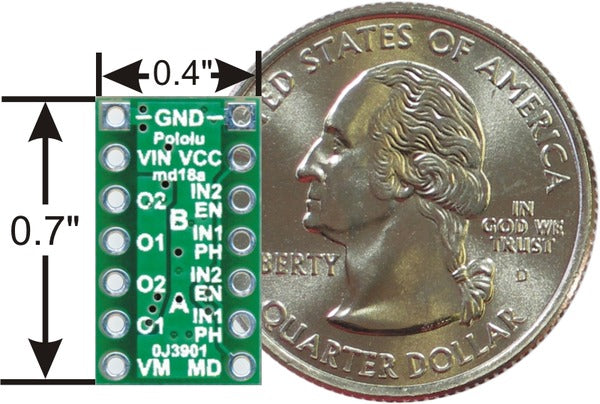
- Compact size (0.7″×0.4″) with the form factor of a 14-pin DIP package
Using the motor driver
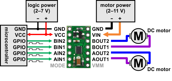
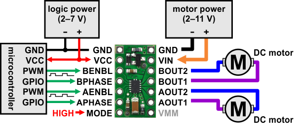 |
| Minimal wiring diagram for connecting a microcontroller to a DRV8835 dual motor driver carrier in phase-enable mode. |
|---|
Motor and motor power connections are made on one side of the board and logic power and control connections are made on the other. Each control input is pulled low through a weak pull-down resistor (approximately 100 kΩ), so the driver will be in the IN/IN mode if the MODE pin is left disconnected, and the driver outputs will be disabled by default. The driver requires a motor voltage between 2 and 11 V and a logic voltage between 2 and 7 V; the logic voltage can typically be supplied by or shared with the controlling device.
The DRV8835 features two possible control modes: IN/IN and PHASE/ENABLE. The MODE pin determines the control interface. Setting the MODE pin high, either with a pull-up resistor or a driving-high I/O line, sets the driver to PHASE/ENABLE mode, where the PHASE pin determines the motor direction and the ENABLE pin can be supplied with a PWM signal to control the motor speed. This mode is generally easier to use as it only requires one PWM per channel, but it only allows for drive/brake operation. (Drive/brake operation usually provides a more linear relationship between PWM duty cycle and motor speed than drive/coast operation, and we generally recommend using drive/brake operation when possible.)
| Simplified drive/brake operation with MODE=1 (PHASE/ENABLE) | ||||
|---|---|---|---|---|
| xPHASE | xENABLE | xOUT1 | xOUT2 | operating mode |
| 1 | PWM | L | PWM | reverse/brake at speed PWM % |
| 0 | PWM | PWM | L | forward/brake at speed PWM % |
| X | 0 | L | L | brake low (outputs shorted to ground) |
Advanced usage with IN/IN mode
 |
| Minimal wiring diagram for connecting a microcontroller to a DRV8835 dual motor driver carrier in in-in mode. |
|---|
When the MODE pin is disconnected or low, the control interface is IN/IN, which allows for slightly more advanced control options. The following truth table show how to achieve drive/coast and drive/brake operation using the IN/IN control interface:
| Drive/coast or drive/brake operation with MODE=0 (IN/IN) | ||||
|---|---|---|---|---|
| xIN1 | xIN2 | xOUT1 | xOUT2 | operating mode |
| 0 | 0 | OPEN | OPEN | coast (outputs off) |
| 0 | PWM | L | PWM | reverse/coast at speed PWM % |
| PWM | 0 | PWM | L | forward/coast at speed PWM % |
| PWM | 1 | L | PWM | reverse/brake at speed 100% − PWM % |
| 1 | PWM | PWM | L | forward/brake at speed 100% − PWM % |
| 1 | 1 | L | L | brake low (outputs shorted to ground) |
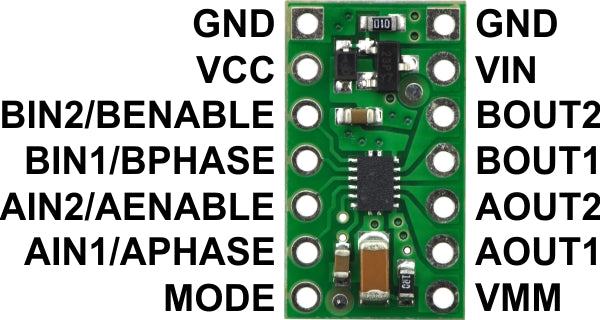
Pinout
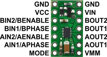 |
| PIN | Default State | Description |
|---|---|---|
| VIN | 2–11 V motor power supply connection. Operation at low VIN voltages slightly reduces the maximum current output. | |
| VCC | 2–7 V logic power supply connection. This should be at or near the logic voltage of the control signal source. | |
| VMM | This pin gives access to the motor power supply after the reverse-voltage protection MOSFET (see the board schematic below). It can be used to supply reverse-protected power to other components in the system. It is generally intended as an output, but it can also be used to supply board power. | |
| GND | Ground connection points for the motor and logic power supplies. The control source and the motor driver must share a common ground. | |
| AOUT1 | The motor A half-bridge 1 output. | |
| AOUT2 | The motor A half-bridge 2 output. | |
| BOUT1 | The motor B half-bridge 1 output. | |
| BOUT2 | The motor B half-bridge 2 output. | |
| AIN1/APHASE | LOW | A logic input control for motor channel A. |
| AIN2/AENABLE | LOW | A logic input control for motor channel A. |
| BIN1/BPHASE | LOW | A logic input control for motor channel B. |
| BIN2/BENABLE | LOW | A logic input control for motor channel B. |
| MODE | LOW | Logic input that determines the control interface. Logic low on this pin results in IN/IN mode while logic high results in PHASE/ENABLE mode. |
Real-world power dissipation considerations
The DRV8835 datasheet recommends a maximum continuous current of 1.5 A per motor channel. However, the chip by itself will overheat at lower currents. For example, in our tests at room temperature with no forced air flow, the chip was able to deliver 1.5 A per channel for approximately 15 seconds before the chip’s thermal protection kicked in and disabled the motor outputs, while a continuous current of 1.2 A per channel was sustainable for many minutes without triggering a thermal shutdown. The actual current you can deliver will depend on how well you can keep the motor driver cool. The carrier’s printed circuit board is designed to draw heat out of the motor driver chip, but performance can be improved by adding a heat sink. Our tests were conducted at 100% duty cycle; PWMing the motor will introduce additional heating proportional to the frequency.
This product can get hot enough to burn you long before the chip overheats. Take care when handling this product and other components connected to it.
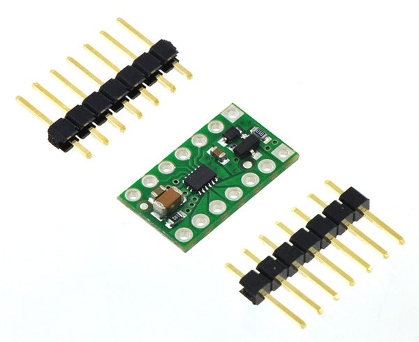
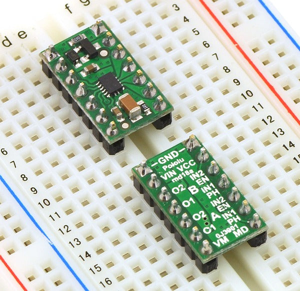
Included hardware
|
|


Two 1×7-pin breakaway 0.1″ male headers are included with the DRV8835 dual motor driver carrier, which can be soldered in to use the driver with perfboards, breadboards, or 0.1″ female connectors. (The headers might ship as a single 1×14 piece that can be broken in half.) The right picture above shows the two possible board orientations when used with these header pins (parts visible or silkscreen visible). You can also solder your motor leads and other connections directly to the board.
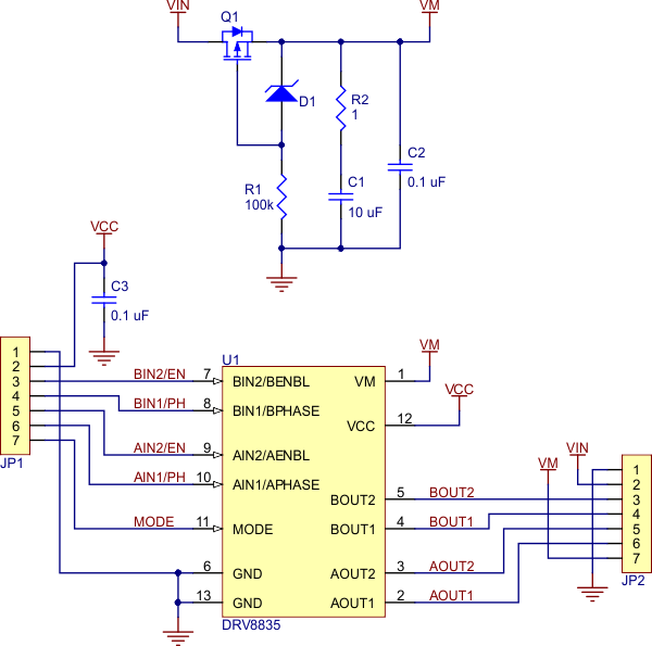
Schematic
 |
| Schematic of the DRV8835 dual motor driver carrier. |
|---|